The schematic was created using DipTrace.
It uses more than 500 pins (mainly due to the replication of µC pins on
the connector headers).
Therefore the DipTrace Lite license (limited to 500 pins) is not
sufficient and at least the Standard License (1000 pins) is needed to
modify the schematic.
As the whole project, it's released under the Creative
Commons CC-BY license. The full schematics in PDF
format can be found here.
For schematics in DIP format, please have a look in the repository.
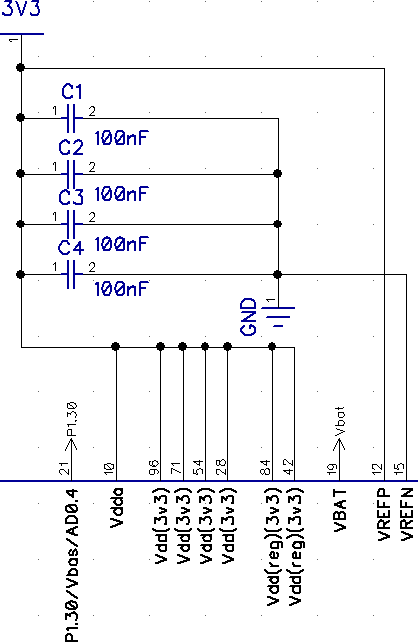
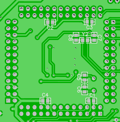
Note that the capacitors shown in parallel here are indeed meant to be as
close to the voltage supply pins in the layout.
Vbat is left open to allow battery supply to the RTC domain (see LPC1768
manual) - even though this is not used.
As long as core power is present, this doesn't make any difference anyway.
Also note that the commercially available Core Board connects Vbat to 3.3V
as well.
When using the Core Board, the capacitors (on the bottom) are not populated.


This is just the default circuit also used on the commercial Core Board.
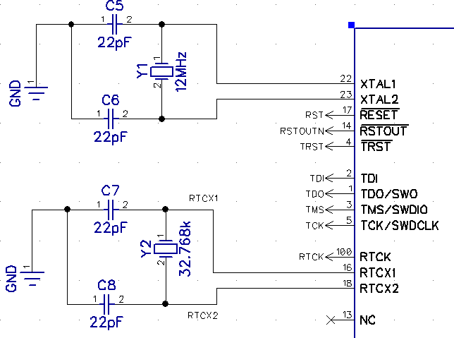
Note that the real time clock oscillator is meant for low power modes,
where only the RTC domain (real time clock) is running and the 32.768kHz
oscillator serves as low power oscillator.
The current software doesn't use any low power modes and there's really no
need, so the pins RTCX1/RTCX2 could also be left floating.
Then again, the Core Board has the RTC oscillator placed and it doesn't
hurt to keep it at least in the schematic and layout as population option.
When using the Core Board, neither the crystals nor the (SMD) capacitors (on the bottom) are populated.
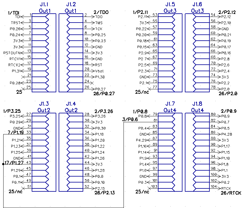
The headers allow connection to the commercially available Core Board.
Therefore the pin assignment replicates that of the Core Board.
All pins are replicated on the four 26pin headers but the main Xtal pins.
The only difference in pinning is that the Vbat pin is not connected to
3.3V - which is the case on the Core Board.
Also note that P0.6 (MAT2.0) is directly connected to P1.19 (CAP1.1) and
P1.27 (CAP0.1).
This is the connection needed to use Timer0 and Timer1 as counters driven
by a clock created by Timer2 (angle tick timer).
When using the Core Board, the header is needed as connection to the board. If the µC is directly placed on the PCB, the headers are optional (e.g. for measuring or extension).
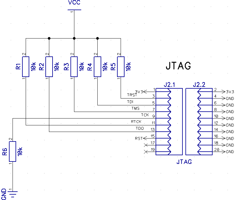
The JTAG interface used for debugging and reprogramming the bootblock. Just default circuit for ARM Cortex-M3.
When using the Core Board, neither the JTAG header nor the (SMD) resistors are populated.
The Schottky rectifier 1N5819 serves as reverse voltage protection. J9 is
a screw terminal connected to the main power switch.
The regulators L4940 (5V) and LF33CV (3.3V) are chosen for easy
availability. For both of them, the recommended application circuits are
used.
I had concerns that connecting the input capacitor of the LF33CV directly
in parallel to the output capacitor of the L4940 could have an impact on
the 3.3V regulation, but I couldn't observe any negative impact.
Note that when using the commercial Core Board, the output of its own
(inactive) 3.3V regulator (LM1117-33) is directly connected to the output
of the LF33CV.
I was concerned if this could cause unexpected behavior e.g. due to
reverse current flowing into the LM1117-33. However after studying its
block diagram this seemed unlikely and also testing didn't show any
effects.

The idea from the beginning was to have a push-pull output for each of
the four channels with 100mA continuous current on each output.
Surprisingly, there are not many choices with good availability. There are
of course dozens of CMOS buffers/drivers like the 74HCT125.
However, most of them have very limited current ratings (e.g. maximum
supply pin rating of 50-70mA) which makes them useless for this
application.
I also thought about using multiple CMOS latches with outputs connected in
parallel to increase the current capability.
Then again, this would have increased the size of the output circuit quite
a bit (and thus the cost of the PCB) and besides, connecting CMOS outputs
in parallel can increase the chance of latchup.
In the end I found the TC446x family by Microchip and chose the TC4469
mainly because of good availability. The TC4469 is a quad push-pull driver
two inputs (AND) per output, where one of the inputs is inverted.
While this 2nd input per channel was not really something I was looking
for, I decided to connect all the inverted inputs and use them as common
disable line for the outputs. So the 20k pullup R8 disables the outputs as
long as the µC doesn't pull P1.24 low.
The diodes 1N5908 are unidirectional "Transil" clamping diodes used for
overvoltage protection (short circuit to power).
The 100k pulldowns are used to get a defined ground level on the outputs
if the driver is off.
PFRA is a polyfuse to limit current through the series resistors and the
clamping diodes in case of overvoltage (short circuit to power).
The 39Ohm resistors are rated 2W to withstand the current in an
overvoltage scenario until the polyfuse trips. Note that 39Ohm is chosen
since the polyfuse adds ~3Ohm to the output impedance and the quad driver
adds ~10Ohm. In sum, the output impedance should be ~51Ohm.
It's important to note that the supply of the quad driver is not directly
connected to 5V, but to a separate net called 5VPROT.
This is because the clamping diodes can't guarantee a 5V level in an
overvoltage condition and a clamping voltage of ~7V would be connected to
the 5V net when the highside of one of the four push-pull stages inside
the quad driver was connected to ground.
Instead, the clamping voltage is connected to 5VPROT.
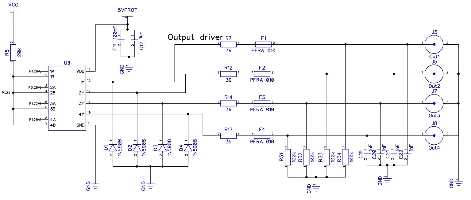
To be able to keep the 7V clamping voltage in an overvoltage scenario
away from the main 5V net, a P-FET is used which is switched off
automatically if 5VPROT raises over ~5.1V.
The details are described in Output
Protection.

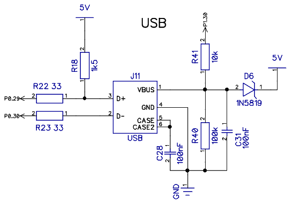
Pretty much a default circuit with the recommended 33 Ohm series
resistors. P1.30 is the µC's VBus input which enables the µC to detect the
presence of USB bus power.
The Schottky rectifier 1N5819 was meant as reverse voltage protection when
powering the device via USB.
It is not recommended to place it though as it bypasses the main power
switch and also decreases the output voltage to ~4.5V (also the LCD
contrast and backlight brightness is lowered).
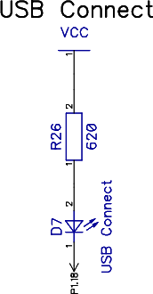
P1.18 is the UP_LED output used for th USB GoodLink feature: when
the device is successfully enumerated and configured, the LED is
permanently on (UP_LED is driven low). During suspend, the LED is off.
Note: in a future version, the diode D6 should be either removed or a header should be placed to switch it though the main power switch.
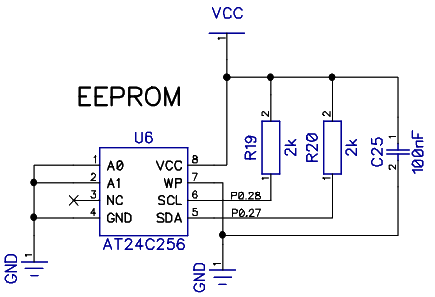
Nothing surprising here. Typical 2k pullups for the I2C bus. Address
lines pulled to ground → 0.
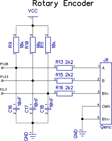
A rotary
encoder (Bourns PEC16 2215F-S002) with push button is used as manual
input option for setting the engine speed.
P1.20 (MCI0) and P1.23 (MCI1) are connected to the quadrature encoder
interface (QEI) of the µC which allows automatic position tracking in
hardware.
Even though the QEI has a digital deglitch filter, the input circuit
serves as additional lowpass filter (τ = 22µs).
Note that while turning, the rotary encoder will shortly connect the lines
A and B to the common connector (CMN) which is connected to ground.
So the serial 2k2 resistors will only smoothen the signal's falling edge.
A soon as the connection to ground is removed, the capacitors will be
charged via the 10k pullups.
So the filtering of rising and falling edges is a little unsymmetrical.
This is however necessary as the 10k pullup and the 2k2 series resistor
form a voltage divider.
If both had the same value, the voltage would be only halved (3.3V/2 =
1.65V) when A/B are connected to CMN/GND.
As the threshold for low level detection is ~0.8V, this would make it
impossible to detect a low level. Using 2k2 and 10k, the low level is
decreased to ~0.6V (3.3V*2.2/(10+2.2) = 0.595V), which is safe enough
below the low level threshold and still keeps the falling egde filtering
functional.
P2.11 is an interrupt input (EINT1) used to detect button presses of the
rotary encoder (Btn is connected to Btn- if the rotary encoder is pushed
down).
This pin is also used to enter the USB boot loader during power up (so the
rotary encoder button has to be pushed down while the device is switched
on to enter the USB boot loader).
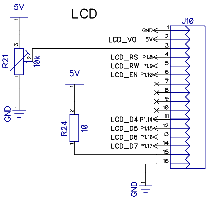
A configuration with 4 parallel data lines (P1.14 - P1.17) is used.
Control lines RS/RW/EN are connected to the same port.
The 10 Ohm resistor is used to limit the current into the LED backlight
(even though with most LCD modules, this is not really needed).
The potentiometer R21 is used to set the contrast of the LCD.
The connector matches that of a typical 16x2 LCD module with Hitachi
HD44780 compatible controller.
The idea is to directly solder the LCD to the PCB via a right angle
header.
A MAX202 is used instead of a classic MAX232 since it requires only 100nF
resistors for its charge pumps.
Of course any other pin compatible clone can be used as long as it's ok
with 100nF resistors.
Indeed the MAX202 (as the MAX232) is a dual channel transceiver where only
one channel is used and there are also parts available which feature only
one channel.
Again, the dual channel MAX202 was mainly chosen for good availability.
UART1 is used: P2.0 is TXD1 and P2.1 is RXD1.
The header on the PCB is designed to allow a flat cable connection to a D-Sub connector for flat ribbon cable:
| D-Sub | Header | |
| TX | 2 | 3 |
| RX | 3 | 5 |
| GND | 5 | 9 |
Note that the UART is currently not actively used. It was meant for
debugging or as future extension in combination with the CAN (LAWICEL).
Unfortunately, reprogramming the device via the serial bootloader is only
possible via UART0, while the current hardware uses UART1 - mainly because
this made routing easier.
For a future update, it would make sense to move the UART to UART0 - but this makes routing a bit tricky.

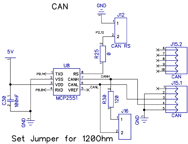
The transceiver used is as Microchip MCP2551 - selected again only for
good availability.
P0.0 is RD1, P0.1 is TD1. VREF output (reference voltage = VDD/2) is
not used and left open.
Using jumper J16, it is possible to connect a 120Ohm terminator.
Through jumper J12 and the placement of R25, it is possible to connect the
RS input (slope control) directly to ground or use a different resistor.
Note that RS has to be pulled to GND for high speed mode - at high
level (also if the input is floating) set the transceiver to sleep mode.
The pin P2.12 is meant to allow switching between ground and sleep mode
through software.
If this feature is used and P2.12 is driven low, the jumper J12 must be
left open to avoid a short circuit to ground.
As for the UART, the header on the PCB is designed to allow a flat cable connection to a D-Sub connector for flat ribbon cable:
| D-Sub | Header | |
| CANH | 7 | 4 |
| CANL | 2 | 3 |
| GND | 3, 6 | 5, 2 |
Note that CAN is currently not used - and indeed not even tested.
Currently this is just an option for future CAN functions.
